

Automotive Shunt Resistor Manufacturer Reveals Key Design Tips for High-Precision EV Current Sensing
2026-09-07
Getting accurate current readings in an EV is harder than most engineers expect—thermal drift, shunt placement, and even PCB layout can silently erode precision. Milliohm, a dedicated automotive shunt resistor manufacturer, shares field-tested design tips that go beyond datasheet numbers. From material selection to Kelvin connection pitfalls, here's what actually moves the needle in high-precision EV current sensing.
Thermal EMF at Dissimilar Metal Junctions Distorts Low Current Measurements
Any junction between two different metals behaves as a thermocouple. If the two ends of that junction sit at slightly different temperatures, a small voltage appears in the circuit. For low-current measurements this voltage becomes problematic because even a microvolt-level offset can flow through a high-value resistor or the high output impedance of a device under test and masquerade as a real current. Copper-to-tin/lead solder, for instance, can produce a thermal EMF of roughly 1–3 µV per °C. A temperature difference of just 0.1 °C across such joints can easily inject hundreds of nanovolts into a measurement loop—enough to shift a picoamp-level reading by a noticeable amount.
In practical setups, low-current paths pass through binding posts, relays, connectors, PCB traces, and internal wiring. Every transition from one conductor material to another adds another thermocouple junction. The temperature gradients that drive thermal EMF are also harder to avoid than they first appear. They don't require an obvious heat source; heat dissipated by nearby regulators or power supplies, proximity of an operator's hand, and even slow room-air convection can create stable but small temperature differences. Because low-current instruments often convert current to voltage across a known resistance, any unwanted voltage in series with that resistance is interpreted as a current offset. This is particularly harmful at the high-impedance summing node of a feedback ammeter, where thermal EMF across the input connection directly cancels or adds to the measured signal.
Reducing the effect starts with the physical construction of the measurement loop. Keep all connections made of similar metals close together so they share nearly the same temperature. Use connectors and relays specified for low thermal EMF, and avoid introducing unnecessary metal transitions in sensitive lines. Let the entire instrument and test fixture reach thermal equilibrium before taking data, and shield the setup from drafts or localized heating. For the most demanding measurements, reversal and nulling techniques work better than trying to estimate the offset once. Reversing the current direction or opening the input and measuring the residual voltage lets you separate the real signal from the standing thermal voltage. Just remember that the offset drifts with any change in the thermal environment, so a one-time subtraction is only reliable when temperatures remain stable.
Four-Terminal Kelvin Sensing Layouts That Eliminate Trace Resistance Errors
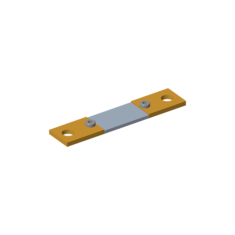
A four-terminal Kelvin layout works because it splits the current path from the voltage sense path so the voltage drop across PCB traces never contaminates your reading. In practice, that means running a dedicated pair of force traces to carry the excitation current, and a separate pair of sense traces that tap directly at the component pads. Because the sense lines only connect to a high-impedance input, almost no current flows through them. That keeps their own trace resistance out of the equation, even if the sense routes are long or thin compared with the force routes.
A clean Kelvin connection starts at the footprint. For a two-terminal sense resistor, the ideal layout splits each pad into two separate copper areas: one for the force connection and one for the sense connection. The sense trace should leave from the inner edge of the pad, as close to the resistive element as possible, while the force trace connects on the outer edge. Any copper that is shared between the force path and the sense tap will introduce a small IR drop, and that shared segment becomes a direct error source. Keeping the sense vias out of the main current path and routing the sense pair as a tight differential pair also reduces coupling from nearby switching nodes.
When the layout is done this way, trace resistance errors are largely removed from low-value measurements. The approach is especially useful for current-sense resistors in power converters, battery fuel gauges, and precision milliohm metering, where a few milliohms of trace resistance can swamp the signal. The result is repeatable readings that depend on the component itself rather than on board thickness, copper weight, or soldering variations.
Why Resistance Tolerance Is a Poor Predictor of Real World Drift
Resistance tolerance is often treated as a stand-in for how much a resistor will shift over time, but that assumption breaks down quickly in real circuits. The tolerance figure on a datasheet describes the allowable spread of initial resistance values coming off the production line—it says nothing about what happens after the part leaves the factory. A 1% resistor might start within 1% of its marked value, yet drift 5% or more over a few years of thermal cycling, humidity exposure, or even mild overload. The gap between initial accuracy and long-term stability is where many designs quietly fail.
Part of the problem is that drift mechanisms don't map to the same variables that set initial tolerance. Thin-film resistors may have tight initial tolerances but can be more sensitive to moisture ingress or electromigration than thick-film types with looser tolerances. A precision resistor with 0.1% tolerance can exhibit surprisingly large reversible shifts from moisture absorption, while a cheap carbon film part might hold steady under the same conditions. Tolerance only tells you the starting line, not the direction or distance the resistance will travel.
Real-world drift also accumulates from stress factors that no static tolerance spec can anticipate—pulse loads, board flexure, chemical contamination, and even soldering heat can permanently alter the resistive element. When engineers rely on tolerance as a predictor, they're essentially assuming the resistor will stay near its initial value, but drift is a different physical process with its own time constants and failure modes. The result is that a circuit can pass incoming inspection with perfectly in-tolerance parts and still fall out of spec months later, not because the parts were bad, but because tolerance was never meant to predict that kind of change.
Pulse Power Handling Without Sacrificing Long Term Stability
High pulse power tolerance isn't simply about surviving a transient spike—it's about doing so repeatedly without degrading the material's inherent stability. Many components rated for high peak power drift after a few hundred cycles, their resistance or capacitance values shifting due to micro-structural fatigue. A well-engineered part addresses this by using thick-film or wirewound elements with low thermal coefficient and even heat distribution, ensuring each pulse dissipates evenly across the surface rather than concentrating at weak points. This reduces hot spot formation, the primary cause of long-term parameter shift.
Beyond basic survivability, the key is matching the pulse energy to the element's thermal mass. Rather than relying on oversized margins that sacrifice board space, the design uses a balanced approach: the element absorbs and releases heat quickly enough to handle rapid pulse trains, yet retains enough thermal inertia to avoid sudden temperature spikes that accelerate aging. The result is a component that holds its rated tolerance after thousands of high-energy pulses, without the gradual creep that plagues lower-grade alternatives.
Solder Joint Creep and Board Strain as Overlooked Accuracy Killers
Solder joints aren't rigid anchors; under sustained mechanical load or elevated temperatures, they slowly deform through creep. In precision analog front-ends, even a few microstrains of creep displacement can shift the relative position of a shunt resistor or reference node, altering parasitic inductance and resistance just enough to corrupt a 24-bit ADC's last three digits. This drift rarely shows up in short bench tests, so it gets written off as unexplained noise or blamed on firmware.
Board strain is equally insidious. When a PCB flexes due to mounting screws, thermal expansion mismatches, or connector insertion forces, that bending transfers directly into sensitive components—especially ceramic capacitors and MEMS sensors. A strain of 300 με across a X7R cap can produce a reversible capacitance change of over 5%, which in a timing or filter circuit translates to frequency errors far beyond the datasheet tolerance. Many designers focus on component specs while ignoring how the board itself acts as a mechanical amplifier.
The combined effect is worst in high-channel-count systems: one warped rail or uneven heatsink clamp creates a strain gradient, and each solder joint along that gradient creeps at a slightly different rate. Over months, the differential creep accumulates into measurable offset voltages and gain mismatches between channels. Field failures often get misattributed to aging or drift, when in reality the root cause is a mechanical boundary condition that was never simulated.
Matching Shunt Resistance to Delta-Sigma ADC Full Scale for Cleaner Signals
Selecting a shunt resistor that aligns with the full-scale input range of a delta-sigma ADC is more than a matter of picking a convenient value. When the voltage drop across the shunt at maximum expected current sits comfortably inside the ADC's differential input span, the converter's inherent noise shaping can work in your favor. Too large a shunt forces the modulator into clipping, while too small a shunt wastes precious signal swing and leaves the low-level codes underutilized. The sweet spot is where the peak shunt voltage reaches roughly 80 to 90 percent of the ADC's specified full scale, leaving a small margin for overloads and component tolerances.
Matching the shunt to the ADC also demands attention to the reference voltage and gain settings. Many delta-sigma converters offer programmable gain amplifiers ahead of the modulator; choosing the right gain keeps the shunt's thermal noise below the ADC's own noise floor without sacrificing headroom. For a clean measurement, the shunt resistance should produce a full-scale voltage that, after gain, lands just under the reference voltage divided by the oversampling ratio's effective range. This avoids the harsh clipping artifacts and the uneven quantization noise that appear when the modulator saturates.
Practical designs often iterate between shunt power dissipation, available standard resistor values, and the ADC's differential input impedance. A shunt that runs too hot drifts and injects thermal EMF into the signal path, while one that is too cold leaves the ADC's least significant bits bouncing on system noise. By plotting the expected current range against the ADC's noise-free resolution, you can pick a shunt that keeps the signal clean across the full dynamic range and avoids the subtle distortion that creeps in when the input stage operates too close to its rails.
FAQ
Shunt resistors deliver a linear voltage drop across a known resistance, so accuracy stays predictable over a wide temperature range. Hall sensors can drift with ambient magnetic fields and require periodic offset correction. In high-vibration automotive environments, a passive metal alloy shunt also tends to be more robust and easier to integrate into busbar designs.
Thermal EMF arises when the junction between the resistive element and the copper lead sees a temperature gradient. That small DC voltage offsets the measured signal and becomes significant at low current levels. Using low-thermal-EMF alloys like manganin, keeping sense connections isothermal, and placing the shunt away from hot spots all help suppress the effect.
With very low resistance values—often 50 to 200 micro-ohms in EV applications—the resistance of PCB traces and solder joints can exceed the shunt itself. A Kelvin layout separates the current-carrying path from the voltage-sensing path, so the measurement only sees the voltage across the resistive element, not parasitic lead resistance.
The resistance should be low enough to limit self-heating and voltage burden, but high enough to produce a measurable signal at the lowest current of interest. The power rating must cover the worst-case continuous RMS current plus transient peaks, with derating for elevated under-hood temperatures. A common approach is to target 50–75% of rated power at maximum continuous load.
Route the Kelvin sense traces as a tightly coupled differential pair, away from switching nodes and high-current paths. Keep the shunt close to the sensing amplifier to reduce loop area. Balance thermal relief so both sense terminals stay at similar temperatures, and avoid placing the shunt near power inductors or MOSFETs that create hot gradients.
Manganin offers very low thermal EMF and good stability but has a relatively high TCR unless compensated. Zeranin and Evanohm provide lower TCR over a wider temperature range but can be more expensive. Copper-manganese-nickel alloys balance cost and performance for volume EV production, while pure nickel alloys suit high-temperature environments if some TCR error is acceptable.
Conclusion
Designing shunt resistors for high-precision EV current sensing demands attention to subtle physical effects that can quietly corrupt low-level measurements. The thermal EMF generated at junctions between dissimilar metals, for instance, creates spurious voltages that distort readings in the milliamp range, so material selection and thermal balancing become critical. Likewise, moving to a four-terminal Kelvin layout does more than reduce trace resistance—it decouples the current path from the sense path, ensuring that only the voltage drop across the resistive element reaches the measurement front end. Experienced engineers also know that a tight initial resistance tolerance says little about long-term stability; real-world drift arises from load cycling, humidity, and oxidation, which is why alloy composition and passivation often matter more than the datasheet tolerance figure.
Beyond DC accuracy, pulse power handling forces a compromise between short-term thermal mass and long-term material fatigue. A shunt that survives a 10-millisecond overload may still degrade if repeated pulses cause microstructural changes, shifting resistance permanently. Then there are the mechanical culprits: solder joint creep under temperature swings and board strain from mounting or vibration introduce variable contact resistance that no amount of signal conditioning can fully remove. Finally, matching the shunt resistance to the delta-sigma ADC's full-scale input range avoids wasted dynamic range and keeps noise floor low, allowing cleaner conversion of small sense voltages into usable digital codes without overdriving or underutilizing the converter.
Contact Us
Contact Person: Yuying Gao
Email: [email protected]
Tel/WhatsApp: +86 18926013721
Website: https://en.milliohm.net/